Advanced Semiconductor Packaging Market Could Reach $80 Billion by 2033 as AI Chips Spread to Consumer Devices, According to Bloomberg Intelligence
October 27, 2025
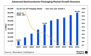
New report shows 2.5D and 3D packaging market could grow 26% annually, outpacing overall chip industry growth as AI moves from data centers into PCs, smartphones and vehicles
TSMC expected to maintain leadership while outsourced assemblers, such as ASE and Amkor, likely positioned to double market share to 16% by 2033
NEW YORK, October 27, 2025 – A new report from Bloomberg Intelligence (BI) finds that the market for advanced semiconductor packaging could grow eightfold to $80.5 billion by 2033, driven by the spread of AI chips from data centers into consumer electronics and automotive applications. The 26% compound annual growth rate significantly outpaces the 10% projected growth for the overall semiconductor industry.
In this special report, Bloomberg Intelligence’s interactive model calculates the addressable market size for 2.5D and 3D packaging technologies that can fit more computing power into each chip, move data faster and use less energy. Advanced packaging technologies, which stack chips vertically or connect them side by side to boost performance and efficiency, are emerging as a critical growth engine as traditional transistor shrinking delivers diminishing returns. The shift represents a fundamental change in how the industry achieves performance gains, with packaging innovation now rivaling chip design in importance.
By 2033, BI finds that advanced packaging will reach 90% penetration in PCs, along with all graphics processors and half of smartphone chips. Automotive processors are expected to hit 18% adoption as autonomous driving systems require more computing power in compact, energy-efficient packages.
“Demand for AI is reshaping semiconductor design, pushing innovation inside the package as transistor scaling nears its physical limits,” said Charles Shum, semiconductor analyst at Bloomberg Intelligence and lead author of the report. “Sustaining the AI boom will depend on how quickly semiconductor design can reach high-volume production. Over the next few years, factory buildouts, new materials and policy measures will be critical to determine the adoption speed and competitive positioning among foundries. The most imminent 2026 milestones include Nvidia’s next-gen AI processing starts mass production and Intel’s volume production of its new server processor using Foveros Direct 3D stacking.”
Taiwan Semiconductor Manufacturing Company (TSMC) is expected to maintain its leadership position with over 40% market share, leveraging its integrated model that combines advanced chip fabrication with packaging under one roof. Meanwhile, outsourced assembly and test providers, including ASE and Amkor, are positioned to capture significant share gains as production scales for cost-sensitive consumer applications.
The research shows that contract chip assemblers could expand their advanced packaging market share to more than 15% by 2033 from 8% in 2024. Their advantage lies in cost-efficient fan-out packaging solutions and global manufacturing footprints that appeal to customers seeking supply chain diversification.
Key findings from the report include:
- AI chip package sizes are expected to triple by 2030 as designs incorporate more computing cores and memory stacks.
- Packaging costs for top-end AI chips could climb to nearly $1,300 per chip in 2028 before falling 45% by 2033 as panel-level packaging and mature 3D stacking reset the cost curve.
- Hybrid bonding technology – which creates copper-to-copper connections thousands of times denser than current methods – will become the preferred solution for cloud AI and autonomous driving after 2028.
- Tight capacity is expected to persist through 2027, with broader AI adoption driving the next expansion phase.
The report also examines how geopolitical tensions and export controls are reshaping the competitive landscape. Possible U.S. restrictions on 3D hybrid bonding equipment could limit China to 2.5D technologies, while supply chain diversification is spurring new integrated-packaging clusters in the U.S. and South Korea alongside Taiwan’s established dominance.
The full Advanced Semiconductor Packaging Deep Dive is available to Bloomberg Terminal subscribers who can access the report via {BI DEEP }.
Contact
Alaina Hay
Bloomberg Intelligence
ahay38@bloomberg.net
About Bloomberg Intelligence
Bloomberg Intelligence (BI) research delivers an independent perspective providing interactive data and investment research on over 2,000 companies, 135 industries and all global markets. Our team of over 400 research professionals help our clients make decisions with confidence in the rapidly moving investment landscape. BI analysis is backed by live, transparent data from Bloomberg and more than 600 third-party data contributors that clients can use to refine and support their ideas. Bloomberg Intelligence is available exclusively on the Bloomberg Terminal and the Bloomberg Professional App. Visit us at https://www.bloomberg.com/professional/product/bloomberg-intelligence/ or request a demo.
About Bloomberg
Bloomberg, the global business and financial information and news leader, gives influential decision makers a critical edge by connecting them to a dynamic network of information, people and ideas. The company’s strength – delivering data, news and analytics through innovative technology, quickly and accurately – is at the core of the Bloomberg Terminal. Bloomberg’s enterprise solutions build on the company’s core strength: leveraging technology to allow customers to access, integrate, distribute and manage data and information across organizations more efficiently and effectively. For more information, visit Bloomberg.com/company or request a demo.